The MetroChip Microscope Calibration Standard for SEM, FIB, AFM, Light Microscopy and Metrology Systems
provides an extensive range of targets with periodic features for enhanced calibration down to the 100nm range.
The MetroChip standard is produced with today's nanotechnology demands in mind. It is designed for a long life
use and presents a stable calibration platform. The standard is produced on a 20x20mm chip with a thickness of
750µm. It delivers high contrast images for analytical SEM with minimal charging and combines a huge
calibration range from 4mm down to 100nm.
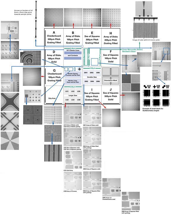
Calibration target for SEM features include alignment marks, linear microscale, distortion measurements,
par-axial calibration (image shift), resolution measurements, focus star, stigmator calibration, gratings,
concentric circles and squares. The combination of these targets on one standard makes the MetroChip ideal
as an all-in-one standard for setting up and regular calibration checks of the SEM, FIB or FESEM. It is also
employed for Light Microscopy and AFM; there are a number of targets to check linearity, distortion and scan length.
The Microscope MetroChip Calibration Target is fully traceable to NIST Certification:
Certification: Traceability of Sample Pitch
Report of Calibration NIST Test No. 821/271639-05
Click here to see overall higher resolution of image below
or click on individual micrographs below to see specific area enlargements.
- Suitable for light microscopy, SEM, FIB, AFM and other metrology systems
- Large range of calibration, from a 4mm ruler down to 100nm geometrics
- Large array of features in both positive and negative structures
- 150nm feature depth with 90° wall angles
- Ease of navigation with dimension labels on most features
- High contrast images in Analytical SEM
- Minimal Charging
- Long Sample Life
- Sample size is 20 x 20mm
- Sample thickness is approximately 750 microns
- The finished product has patterns of etched polycrystalline silicon over a thin oxide on silicon substrate
- Polysilicon thickness is 150nm ±10%
- Oxide thickness under the polysilicon features is less than 5nm, typically 2.5 to 3nm
Metrochip Chip Cleaning Procedure (70KB PDF)
MetroChip Product Description Guide (2.9MB PDF)
Due to an unforseen manufacturing interruption,
the MetroChip Calibration Target is
TEMPORARILY UNAVAILABLE.