Manufacturing Method
PELCO® Silicon Nitride Support Films are manufactured using the latest,
patented, state-of-the-art semiconductor and MEMS manufacturing
techniques. The thin amorphous silicon nitride film is grown on a 200µm thick silicon
wafer to the desired membrane thickness of 8, 15, 35, 50, 100, or 200nm.
The specimen viewing area is created by etching away a window in
the silicon wafer substrate underneath the
Silicon Nitride membrane,
leaving a perfectly smooth, resilient and chemically robust
silicon nitride film. The membrane is not supported in the window area, enabling
large viewing areas without any disturbing
bars. After finishing the window etching process, the individual frames with the
membranes are lifted from the wafer. Wafers used are P-type (B doped) with a resistivity of 2-15 ohm-cm.
Window sizes and shape:
Five single window sizes are available:
- 0.25 x 0.25mm, most robust membrane and most cost effective
- 0.5 x 0.5mm, sturdy and cost effective
- 0.75 x 0.75mm, less fragile, relatively large membrane
- 1 x 1mm, larger area, but more fragile
- 1.5 x 0.5mm, resilient for large viewing area or tomography
Two multiple window sizes are available:
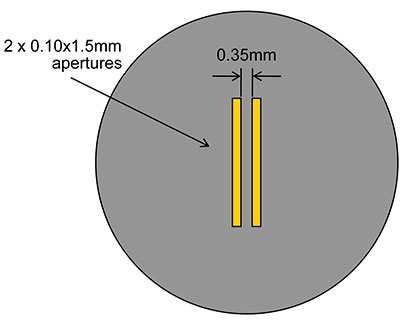
- 2 each 0.1 x 1.5mm, rectangular window
- 3 x 3 array of 0.1 x 0.1mm window
Window with apertures for 8 and 35nm:
- 200nm silicon nitride support mesh
- 25 ea. 60 x 60µm apertures with 8nm membrane; 25 ea. 70 x 70µm apertures with 35nm membrane
- Total window size 0.5 x 0.5mm
Due to the structure of the silicon and the etching process the window in the silicon
substrate is etched with a 35°
angle, leaving a much larger opening than the membrane window at the back side of
the frame:

Table 1. Window dimensions on standard 200µm frame thickness
|
X dimensions (mm)
|
Y dimensions (mm)
|
Area (mm2)
|
Frame thickness
(µm)
|
Membrane thickness
(nm) |
X Back side opening
(mm)
|
Y Back side opening
(mm)
|
|
0.25
|
0.25
|
0.06
|
200
|
15/50/100/200
|
0.53
|
0.53
|
| 0.5 |
0.5 |
0.25 |
200 |
50/100/200 |
0.78 |
0.78 |
|
0.75
|
0.75
|
0.56
|
200
|
50/100/200 |
1.03
|
1.03
|
|
1
|
1
|
1
|
200
|
50/100/200 |
1.28
|
1.28
|
|
1.5
|
0.5
|
0.75
|
200
|
50/100/200 |
1.78
|
0.78
|
|
1.5
|
0.1
|
2 x 0.15
|
200
|
15/50/100/200
|
1.78
|
0.38
|
|
0.1
|
0.1
|
9 x 0.01
|
200
|
15/50/100/200 |
0.38
|
0.38
|
| 0.5 |
0.5 |
0.09 |
200 |
8 |
0.78 |
0.78 |
| 0.5 |
0.5 |
0.12 |
200 |
35 |
0.78 |
0.78 |

Table 2. Window dimensions on special 50µm thin frame version
| X dimensions (mm) |
Y dimensions (mm) |
Area (mm2) |
Frame thickness
(µm) |
Membrane thickness
(nm) |
X Back side opening
(mm) |
Y Back side opening
(mm) |
| 0.25 |
0.25 |
0.06 |
50 |
50 |
0.32 |
0.32 |
| 1.5 |
0.1 |
2 x 0.15 |
50 |
50 |
1.57 |
0.17 |
| 0.1 |
0.1 |
9 x 0.01 |
50 |
50 |
0.17 |
0.17 |
Frame Dimensions
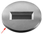
The frame is manufactured as a 3mm silicon disc with smooth EasyGrip™
edges for easy manipulation by tweezers and will fit perfectly in standard TEM holders.
The standard frame thickness of 200µm is more than the typical TEM grid with a
thickness of 15-50µm, but should not present a problem in regular TEM
holders. It is recommended that you check the TEM holders you are using.
For special TEM holder, versions with 50µm frame thickness are available.
50µm frame thickness is compatible with any Ø3mm TEM holder. |
EasyGrip™ Edge
|
Table 3. Manufacturing Tolerances
Manufacturing Tolerances |
| Frame Thickness: |
200µm ±15µm |
|
50µm ±10µm |
|
|
| Membrane Thickness: |
200nm ±10nm |
|
100nm ±10nm |
|
50nm ±5nm |
|
35nm ±4nm |
|
15nm ±3nm |
|
8nm ±2nm |
|
|
| Frame Diameter: |
3.0mm ±0.05mm |
|
|
| Window Dimensions: |
0.1 x 0.1mm (9) - 100µm ±5µm |
|
0.25 x 0.25mm - 250µm ±10µm |
|
0.5 x 0.5mm - 500µm ±20µm |
|
0.75 x 0.75mm - 750µm ±25µm |
|
1.0 x 1.0mm - 1000µm ±30µm |
|
0.1 x 1.5mm (2) - 100µm ±5µm & 1500µm ±40µm |
|
0.5 x 1.5mm - 500µm ±20µm & 1500µm ±40µm |
|
|
| Hydrophilic Coatings: |
2.5nm ±0.25nm |
|
|
| Hydrophobic Coatings: |
2.5nm ±0.25nm |
|
Debris Free Products
Handling capabilities and smoothness of the edges are design advantages over other brands
of silicon nitride support films. The PELCO® Silicon
Nitride Support Films are manufactured like TEM grids with a 3mm diameter using a unique and
patented manufacturing process. They have no broken edges are circular and are completely
free from debris particles unlike other brands of silicon nitride membranes.
The mechanical and chemical stability allow for cleaning or treating of the silicon nitride support
films with chemicals (solvents, acids and bases), glow discharge and plasma cleaning.
It is recommended that ultrasonic cleaning is not be used, as it can easily shatter the
silicon nitride support films.
Effects On Tilt
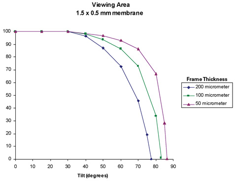
Due to the 35° etching angle the PELCO®Silicon Nitride support films on the frames can be tilted to 35° for unobstructed viewing, even
if the specimen is close to the edge of the membrane. For higher tilting angles,
the specimen needs to be in the center of the membrane. To allow for the highest
possible tilt angle a window size of 1.5 x 0.5mm has been made available, which allows
for tilting angles up to 70° with a viewable area of 40%. Maximum tilt angle
with a specimen in the center, maximum tilt angle is 75°.
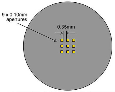
Versions with multiple windows:
- 2 each 0.1 x 1.5mm windows
- 3 x 3 array of 0.1 x 0.1mm windows
This style is made using the
same manufacturing techniques as the single window style Silicon Nitride
membranes. The 200µm frame is available
with 15, 50, 100 and 200nm membrane thickness. The 50µm frame is available with the 50nm membrane thickness.
 |
 |
|
Available for 200 and 50µm substrates with 15, 50, 100 or 200nm silicon nitride membrane thickness.
|
8 and 35nm Membrane Versions
The structure-free 8 and 35nm ultra-thin films are supported by a 200nm mesh, creating 25 apertures.
• 8nm
Silicon Nitride membrane: 60 x 60µm apertures, 35µm bar width, 30µm edge
• 35nm
Silicon Nitride membrane: 70 x 70µm apertures, 25µm bar width, 25µm edge
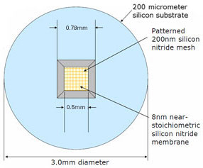
Back Side
|
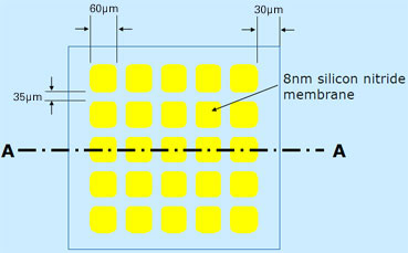
Front Side (enlarged) |
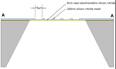
Cross Section View |
- 200µm silicon substrate
- Low stress ultra-thin membranes, close to stoichiometric composition (Silicon Nitride)
PELCO® Holey Silicon Nitride Support Film
All the Silicon Nitride support films are made using the 200nm membrane with a 0.5 x 0.5mm window.