These PELCO® Membranes of Silicon Dioxide (SiO2) offer superior flatness. Using advanced MEMS manufacturing technologies combined with novel stress-reducing techniques, we have been able to provide Silicon Dioxide Support Films with unsurpassed flatness and a membrane thickness of 40nm, 18nm and 8nm. It is truly the next generation Silicon Dioxide membranes. The flatness of our silicon dioxide membranes is at least 10x better than competitive products. The SiO2 membranes are completely amorphous.
Silicon Dioxide Support Films, Product Overview & Manufacturing Details
The Silicon Dioxide (SiO2) Support Films are manufactured using the PELCO® 200nm Silicon Nitride Support Films with the 0.5 x 0.5mm window on a perfectly round 3mm
Si frame as a platform. The silicon dioxide support films consist of pure and amorphous thermal SiO2 membrane. The 0.5 x 0.5mm membrane is patterned into 24 ea. apertures with a size varying between 50 x 50µm to 70 x 70µm and etched back to the thermally-deposited amporhous Silicon Dioxide leaving a structure-free SiO2 thin membrane of 40nm, 18nm or 8nm, suspended by a 200nm optically transparent Silicon Nitride support mesh. The bar
size between the SiO2 apertures is 25-35µm and the boundary width is 25-55µm. The design of the mesh and the ratio of mesh suspension and Silicon Dioxide Film has been optimized to enable flat Silicon Dioxide Support Films with a size of 50 x 50µm to 70 x 70µm. The result is a Silicon Dioxide membrane with a truly superior flatness, ideal for TEM imaging. In the unique design of this PELCO® product, the compression in the SiO2
film is balanced by the stress in the Silicon Nitride grid structure. The mesh size of the Silicon Dioxide Support Films is comparable to the area size found on most 300 and 400 mesh TEM grids and is considered to be a practical size for many applications. There are 24 fields of SiO2 support films on each frame. The boundary of 200nm Silicon Nitride membrane leaves ample area for experiments on Silicon Nitride.
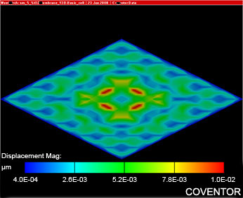
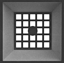
Presentation of film flatness using a simulation for the displacement of SiO2 membrane
versus x-y position on the 0.5mm x 0.5mm window.
|
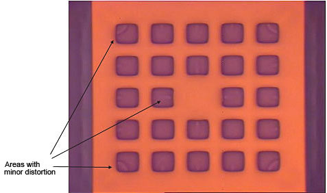
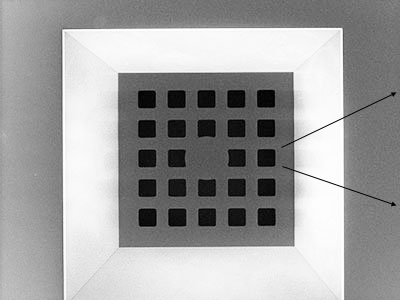
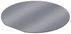
Optical image showing only minor distortion
|
 40nm SiO2 Support imaged from the back with 0.5mm x 0.5mm window etched in ø3mm Si support frame 40nm SiO2 Support imaged from the back with 0.5mm x 0.5mm window etched in ø3mm Si support frame |
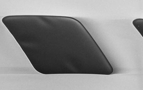 60 degree tilted image of one 50 x 50µm 60 degree tilted image of one 50 x 50µm
Silicon Dioxide Support Film showing smooth surface
|
Thermal Silicon Dioxide is one of most functionalized surfaces in analytical chemistry and can be used as a platform to study base materials and biological entities. The support films can be either used as a passive physical support for TEM imaging or as an active participant in experiments. The PELCO® Silicon Dioxide Support Films have excellent chemical, physical and thermal stability. Properties can be modified or enhanced by coatings, or properties of thin films can be studied by direct deposition on the Silicon Dioxide Film. The 8nm thin SiO2 membranes are resilient enough to allow for manufacturing custom made holes by using an FIB.
Examples of applications are:
- Nanomaterial deposition and growth.
- Thin film analysis and characterization.
- Catalyst research and development.
- Support for FIB lamellae.
- Characterization of semiconductor materials.
- Study of attached biological molecules.
|
8nm SiO2 Support |
Product Specifications
Defining parameters for the PELCO
® Amorphous Silicon Dioxide Support Films are:
Defining parameters for the PELCO
® Amorphous Silicon Dioxide Support Films are:
- Membrane Thickness: 40nm, 18nm and 8nm.
- Aperture Size / Number: 50 x 50µm/24 apertures for 40nm, 60 x 60µm/24 apertures for 18nm and 70 x 70µm/24 apertures for 8nm.
- Pattern: 5 rows x 5 columns with 200nm Silicon Nitride grid support structure, 35µm bar and 55µm edge for 40nm, 35µm bar and 30µm edge for 18nm and 25µm bar and 25µm edge for 8nm..
- Total Window Area: 0.5 x 0.5mm.
- Frame Thickness: Silicon support structure is 200µm standard.
This allows for fitting in standard TEM holders and gives a sturdy support frame.
- Surface Roughness: The RMS (Rq) is 0.65nm which gives a mean roughness (Ra) of 0.41 nm.
- Frame Diameter: TEM standard 3mm diameter disc, fully compatible with regular
TEM holders and with EasyGrip™ edges for improved handling.
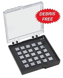
- Packaging: The PELCO® Silicon Dioxide Support Films are packaged under cleanroom conditions. Each box holds 10 support films.
MSDS (360KB PDF)
Made in USA
| Prod #
| Description
| Unit
| Price
| Order / Quote
|
| 21530-10
| Silicon Dioxide Support Film, 40nm, 50 x 50µm apertures (24) on 0.5 x 0.5mm Window, Ø3mm
| pkg/10
| $295.00
|
|
| 21531-10
| Silicon Dioxide Support Film, 18nm, 60 x 60µm apertures (24) on 0.5 x 0.5mm Window, Ø3mm
| pkg/10
| 350.00
|
|
| 8nm thicknesses available soon.
|
| 21532-10
| Silicon Dioxide Support Film, 8nm, 70 x 70µm apertures (24) on 0.5 x 0.5mm Window, Ø3mm
| pkg/10
| 425.00
|
|
Ultra-Flat 6" SiO2 Wafer
5 x 5mm Diced Ultra-flat Thermal SiO2 Substrates
|
Ultra-Flat Thermal SiO2 Substrates
The Ultra-Flat SiO2 substrates consist of a 200nm thermally
grown amorphous SiO2 film on an ultra-flat silicon wafer.
SiO2 is one of the most characterized materials and is widely
used in semiconductor manufacturing, thin film research and as substrate for growing cells. It can be
directly used as substrate for AFM and SEM imaging. The ultra-flat thermal silicon dioxide substrates are
available in 6" wafer and conveniently diced 5 x 5mm, 5 x 7mm and 10 x 10mm chips. The 6" wafer is
shipped in a 6" wafer carrier, the diced pieces are shipped in a Gel-Pak box. The special clean
dicing process involves coating the wafer with photo resist before dicing and removing it after dicing
which produces debris-free SiO2 substratres. All products are
packed in class 10 clean room conditions.
Properties for thermal SiO2 substrates:
- Orientation: <100>
- Grade: Prime / CZ Virgin
- Resistance: 1-50 Ohm/cm
- Type: P / Dopant: Boron
- Wafer Thickness: 655-695 µm
- TTV: <= 7µm / STIR: <= 1.0µm
- Warp: <=40µm / Bow: <= 40µm
- Particles: <=20@>= 3.0µm
- Front surface: Polished
- Back Surface: Etched
- Flat: 1 per SEMI Standard (flat length 57.5+/12.5mm)
- Film: 200nm +/- 5% Thermal Oxide (SiO2), amorphous
- Size: 6" (150mm) diameter wafer or 5 x 5mm, 5 x 7mm or 10 x 10mm diced chips
- Roughness: Typical 2-3 Å
|
|
| Prod #
| Description
| Unit
| Price
| Order / Quote
|
| 21620-6
| 200nm Thermal Oxide on ø6" Ultra-Flat Wafer, Type <100>, in 6" wafer carrier
| each
| $211.65
|
|
| 21620-55
| 200nm Thermal Oxide on 5 x 5mm diced Ultra-Flat Wafer, Type <100>, in Gel-Pak box
| box/25
| 166.70
|
|
| 21620-57
| 200nm Thermal Oxide on 5 x 7mm diced Ultra-Flat Wafer, Type <100>, in Gel-Pak box
| box/18
| 180.00
|
|
| 21620-510
| 200nm Thermal Oxide on 10 x 10mm diced Ultra-Flat Wafer, Type <100>, in Gel-Pak box
| box/6
| 166.70
|
|
|